Organic Field-Effect Transistors

Over the past two decades, solution-processed organic semiconductors have developed into an attractive class of materials for use in flexible and large-area electronic technologies. The main attribute of organic materials for these applications is their soft, flexible nature, together with the ability to print them at low cost over large areas. This may enable the fabrication of novel electronic devices, such as flexible displays for mobile phones or displays integrated into a wide range of everyday objects, including clothing. It might also enable soft, stretchable bioelectronic circuits that can be used in direct contact with human skin to monitor personal health conditions or deliver medical treatments.
To enable such technologies, we work on understanding the charge transport physics of organic semiconductor materials, aiming to elucidate the fundamental charge transport processes in these unusual systems in as much microscopic detail as possible. We work closely with organic chemists to develop new and improved materials and to understand their structure-property relationships. Our work has had some impact on the commercialisation of this technology: we collaborate with industrial partners (such as FlexEnable) to identify and address new requirements and material needs.
Our group has made several pioneering breakthroughs in understanding the fundamental physical mechanisms in organic semiconductors (1,2,3). One example is a recent breakthrough in the development of a printable polymer, in which the natural disorder of individual chains is overcome by a planar and torsion-free polymer backbone. These materials can be imagined as graphene-like tapes, wherein charges can move efficiently along individual chains. As a consequence, the performance of these novel materials is limited by the necessary hopping of charges between polymer chains. We therefore research ways to optimise this process and further improve these materials (4). As a point of reference, the current performance of our easy-to-process polymers already exceeds that of amorphous silicon, which is the material most commonly used in the backplane of liquid crystal displays.

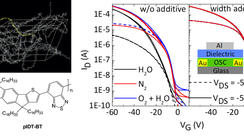
Left: Microstructure and chemical structure of a high-performance polymer. Right: Electrical characteristics of a polymer transistor showing large instability (left panel). The addition of a specific molecular additive results in a drastic increase in stability (right panel).
Besides understanding and improving how charges move in organic semiconductors, we are also interested in how their overall operational stability can be improved. For instance, we recently developed a molecular additive-based technique to significantly reduce the effects of environmental and operational stress in both high-mobility polymer field-effect transistors (FETs) and diodes (5,6). We demonstrated that a major source of instability in conjugated polymers is the presence of small quantities of water within the polymer microstructure: water located between individual polymer chains is incorporated into nanoscale voids. Since these water molecules cannot be easily removed, they act as electron traps, causing degradation of the electrical behaviour. We showed for the first time that stability can be significantly improved by identifying specific molecules that can be inserted into these voids, thereby preventing the infiltration of water. With this approach, we can meet the stability requirements for industrial applications and even match some inorganic technologies. It also enables us to study the intrinsic transport properties of these materials in the absence of trap states.
We are interested not only in organic semiconductors, but also in related carbon-based and hybrid organic–inorganic nanomaterials, such as metal halide perovskites (7), carbon nanotubes, and two-dimensional metal-organic frameworks.
References
- Venkateshvaran, D. et al. Approaching disorder-free transport in high-mobility conjugated polymers. Nature 515, 384–388 (2014).
- Kang, K. et al. 2D coherent charge transport in highly ordered conducting polymers doped by solid state diffusion. Nat. Mater. 15, 896–902 (2016).
- Schweicher, G. et al. Chasing the “Killer” Phonon Mode for the Rational Design of Low‐Disorder, High‐Mobility Molecular Semiconductors. Adv. Mater. 1902407 (2019).
- Thomas, T. H. et al. Short contacts between chains enhancing luminescence quantum yields and carrier mobilities in conjugated copolymers. Nat. Commun. 10, 2614 (2019).
- Nikolka, M. et al. High operational and environmental stability of high-mobility conjugated polymer field-effect transistors achieved through the use of molecular additives. Nat. Mater. 16, 356–362 (2017).
- Nikolka, M. et al. High-mobility, trap-free charge transport in conjugated polymer diodes. Nat. Commun. 10, 2122, (2019).
- Senanayak, S. P. et al. Understanding charge transport in lead iodide perovskite thin-film field-effect transistors. Sci. Adv. 3, 1–11 (2017).
- Senanayak, S. P. et al. A general approach for hysteresis-free, operationally stable metal halide perovskite field-effect transistors. Science Advances 6 (2020).
- Simatos, D. et al. Electrolyte-gated organic field-effect transistors with high operational stability and lifetime in practical electrolytes. SmartMat, 1291 (2024).
- Frisbie, C. D. et al. Charge transport physics of organic conductors at high carrier densities. Nat. Rev. Mater. (2026).
